To reduce parasitic inductances and fully utilize SiC devices, it is crucial to improve the design and architecture of the power system loops.
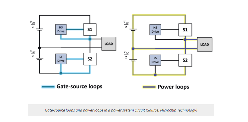
A power system is a complicated network of electrical components that produce, transmit and distribute power to various loads. The gate-source loop and the power loop are the two main loops that make up a power system. The control circuit that powers the switching device, such as an IGBT or silicon carbide MOSFET, is called the gate-source loop. The gate driver, gate resistor, gate capacitance and gate inductance make up the gate-source loop, and the device’s performance and switching speed are set by the gate-source loop.
The primary circuit that transports the load’s voltage and current is the power loop. This loop is made up of the power source, the switching device, the load and parasitic elements like package inductance, PCB trace inductance and stray inductance. Therefore, the power system’s dependability and efficiency are impacted by the power loop.
The loops in the electricity system are linked and impact one another. Both the power loop and the gate-source loop influence how the device switches, and in the power system loops, parasitic inductances can lead to several issues, including switching losses, accidental turn-ons, voltage overshoots and oscillations in the switching process. To reduce parasitic inductances and fully utilize SiC devices, it is crucial to improve the design and architecture of the power system loops.
Sources and consequences of inductive effects
In a power system loop, the inductive effects are caused by the parasitic inductances of the components and the layout. Parasitic inductances are the unwanted inductances that are inherent in any physical conductor. They are determined by the geometry, length and proximity of the conductors. Parasitic inductances can have negative impacts on the power system’s performance and reliability. Some of the common consequences of inductive effects are:
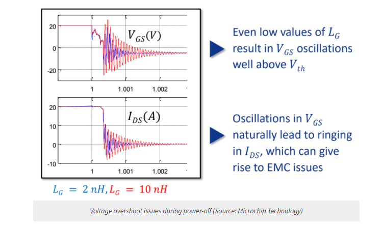
● Voltage overshoot: When the switching device turns off, the current in the power loop cannot change instantaneously due to the parasitic inductance. The parasitic inductance causes a voltage spike across the device, which can exceed its breakdown voltage and damage it.
● Switching oscillations: The parasitic inductance and the device capacitance form a resonant circuit, which can cause ringing at the switch node. The ringing can increase the switching losses, electromagnetic interference and noise sensitivity.
● Inadvertent turn-on: The voltage spike and the ringing can couple to the gate-source loop through the Miller capacitance and cause a false turn-on of the device. This can result in a short-circuit and a shoot-through current.
● Switching losses: The parasitic inductance slows down the switching speed and increases the switching time. This prolongs the transition period when both the voltage and the current are high, which leads to higher switching losses.
Therefore, it is essential to reduce the parasitic inductances in the power system loops to avoid these problems and improve the efficiency and reliability of the power system.
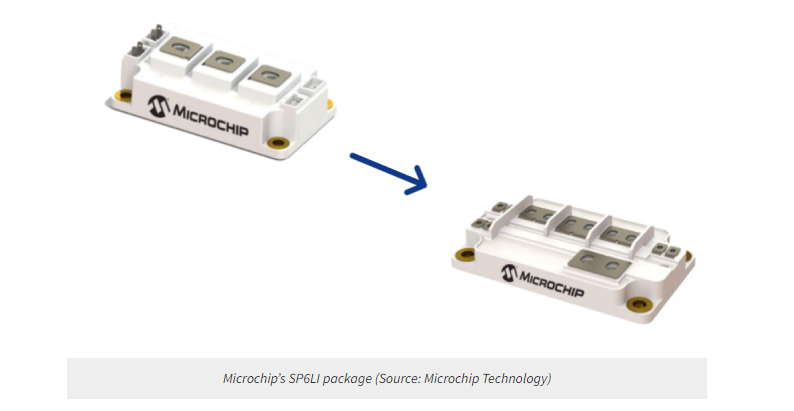
Harnessing SiC capabilities with Microchip’s SP6LI package
SiC devices offer many advantages over conventional silicon devices, such as higher breakdown voltage, lower on-resistance, faster switching speed and higher operating temperature. However, to fully exploit the potential of SiC devices, it is necessary to have a suitable package that can handle the high-current, high-frequency and high-efficiency requirements of the power system.
Microchip’s SP6LI package is a novel solution that is designed to reduce parasitic inductances and unleash the performance of SiC devices. The SP6LI package is a phase-leg module that consists of two SiC MOSFETs and two SiC Schottky diodes in a half-bridge configuration. The SP6LI package has a very low stray inductance of 2.9 nH, which is achieved by using a symmetrical layout, a direct-bond–copper substrate and a low loop area.
The SP6LI package offers several benefits for the power system, such as:
● Lower voltage overshoot: The low inductance of the SP6LI package reduces the voltage spike across the device during turn-off, which protects the device from overvoltage stress and improves reliability.
● Faster switching speed: The low inductance of the SP6LI package enables faster switching transitions and higher switching frequency, which reduces the switching losses and increases the power density.
● Higher efficiency: The low inductance of the SP6LI package minimizes the switching losses and the conduction losses, which improves the efficiency and the thermal performance of the power system.
● Higher power density: The SP6LI package has a compact form factor and a high current rating, which allows a lower quantity of modules in parallel to achieve complete systems, which helps designers to downsize their equipment further.
● Therefore, the SP6LI package is an ideal choice for harnessing the capabilities of SiC devices and enhancing the performance of the power system.
Displaying reduced inductance and illustration of long-term energy conservation
To demonstrate the reduced inductance of the SP6LI package, Microchip has conducted a comparison test with a conventional D3 package under the same conditions. The test results show that the SP6LI package has a significantly lower voltage overshoot and ringing at the switch node than the D3 package, indicating a lower parasitic inductance. The SP6LI package also has a shorter switching time and a lower switching loss than the D3 package, enabling a higher switching frequency and higher efficiency.
The reduced inductance and switching loss of the SP6LI package can translate into long-term energy conservation and cost savings for the power system. Microchip has estimated the energy consumption and the cost of ownership of the SP6LI package and the D3 package for a typical application of a 150-kW three-phase inverter operating at 20-kHz switching frequency and 400-V DC bus voltage. The results show that the SP6LI package can save up to 40% of energy and reduce the cost of ownership by up to 28% compared with the D3 package over a lifetime of 10 years.
About US
Heisener Electronic is a famous international One Stop Purchasing Service Provider of Electronic Components. Based on the concept of Customer-orientation and Innovation, a good process control system, professional management team, advanced inventory management technology, we can provide one-stop electronic component supporting services that Heisener is the preferred partner for all the enterprises and research institutions.