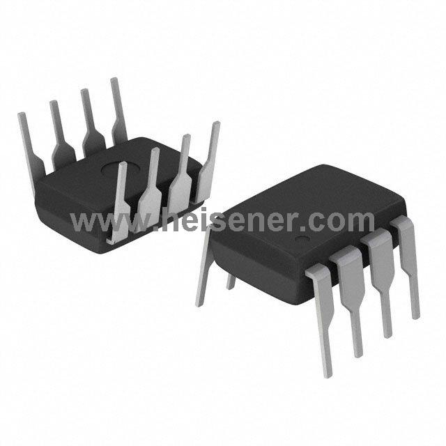
UA741CN Introduction
The UA741CN is a high-performance monolithic operational amplifier built on a single silicon chip, designed for a broad spectrum of analog applications. It features a high gain and operates across a wide range of voltages, making it exceptionally suitable for use in integrators, summing amplifiers, and general feedback circuits.
Additionally, the UA741CN includes an internal compensation network with a slope of 6 dB/octave, which ensures stability in closed-loop configurations. These attributes collectively provide superior performance and reliability, making the UA741CN a versatile and widely utilized component in various electronic and signal processing applications.
UA741CN Pinout

1. Offset Null 1: Used to adjust the offset voltage.
2. Inverting Input (-): Input where the signal is inverted in the output.
3. Non-Inverting Input (+): Input where the signal remains in phase in the output.
4. VCC-: Negative power supply (typically the negative voltage rail).
5. Offset Null 2: Second pin for offset voltage adjustment.
6. Output: The output of the amplifier.
7. VCC+: Positive power supply (typically the positive voltage rail).
8. N.C. (No Connection): This pin is not internally connected.
UA741CN Schematic Diagram

UA741CN Symbol

UA741CN Footprint

UA741CN 3D Model

UA741CN Specification
| Parameter | Specification |
| Input Voltage Range | ±15V |
| Input Offset Voltage | 1 mV |
| Input Bias Current | 10 nA |
| Input Offset Current | 20 nA |
| Supply Current | 1.7mA |
| Output Current | 25 mA |
| Large Signal Voltage Gain | 20,000 V/V (86 dB) |
| Gain Bandwidth Product | 1 MHz |
| Slew Rate | 0.5 V/µs |
| Common-Mode Rejection Ratio | 70 dB |
| Power Supply Rejection Ratio | 86 dB |
| Operating Temperature Range | 0°C ~ 70°C |
| Package Type | 8-DIP |
UA741CN Features
Large input voltage range
No latch-up
High gain
Short-circuit protection
No frequency compensation required
Same pin configuration as the UA709
UA741CN Applications
Summing amplifiers
Voltage followers
Integrators
Active filters
Function generators
Signal summing
UA741CN Package Info
The UA741CN is packaged in an 8-pin Dual In-line Package (DIP), designed for easy mounting in standard sockets or direct soldering onto PCBs. With 8 pins arranged in two parallel rows, this package type is widely used for its durability and compatibility with breadboards. It is ideal for prototyping and various analog circuit applications.
In terms of dimensions, the 8-DIP package of the UA741CN has a standard width of 6.35 mm and a length of 9.27 mm, with a height of approximately 3.3 mm. The pin pitch, or distance between pins, is 2.54 mm, conforming to typical DIP spacing standards, and each pin has a length between 3.0 mm and 3.8 mm. This compact yet accessible layout makes it convenient for integration into designs requiring operational amplifiers for applications like signal conditioning, integrators, or feedback control systems.

How to Connect UA741CN?
Connecting the UA741CN is straightforward. First, place the UA741CN on a breadboard or PCB. Next, connect the power supply to pins 4 and 7 of the chip. Typically, pin 4 (VCC-) connects to the negative power supply, and pin 7 (VCC+) connects to the positive power supply. The usual power range is ±15V, but a lower voltage can be used as needed, as long as it does not exceed the chip's specifications.
Then, determine the input signal connection. Connect the signal to be amplified to either pin 3 (non-inverting input) or pin 2 (inverting input), depending on the circuit requirements. For example, if using a non-inverting amplifier setup, connect the input signal to pin 3 and link pin 2 to ground or a bias voltage to set the correct offset.
Finally, draw the output signal from pin 6, and connect it to the next stage of the circuit or an output device as required. If offset voltage adjustment is needed, use a potentiometer between pins 1 and 5 to achieve zero-offset output. With these steps, the UA741CN is successfully connected and ready to perform amplification or feedback control tasks in the circuit.
FAQs
What is UA741CN?
The UA741CN is a monolithic operational amplifier (op-amp) built on a single silicon chip. Known for its high gain and wide voltage range, it's suitable for various analog applications, including integrators, summing amplifiers, and general-purpose feedback circuits.
Can the UA741CN handle AC signals?
Yes, the UA741CN can process AC signals, making it suitable for audio and AC signal amplification applications. However, for higher frequencies, other op-amps with higher gain bandwidth may be more appropriate.
What is offset null, and how do I adjust it?
Offset null allows you to reduce or eliminate unwanted voltage offsets in the op-amp's output. Adjusting the offset is done by connecting a potentiometer between pins 1 and 5, tuning the potentiometer to achieve zero output when no input signal is present.