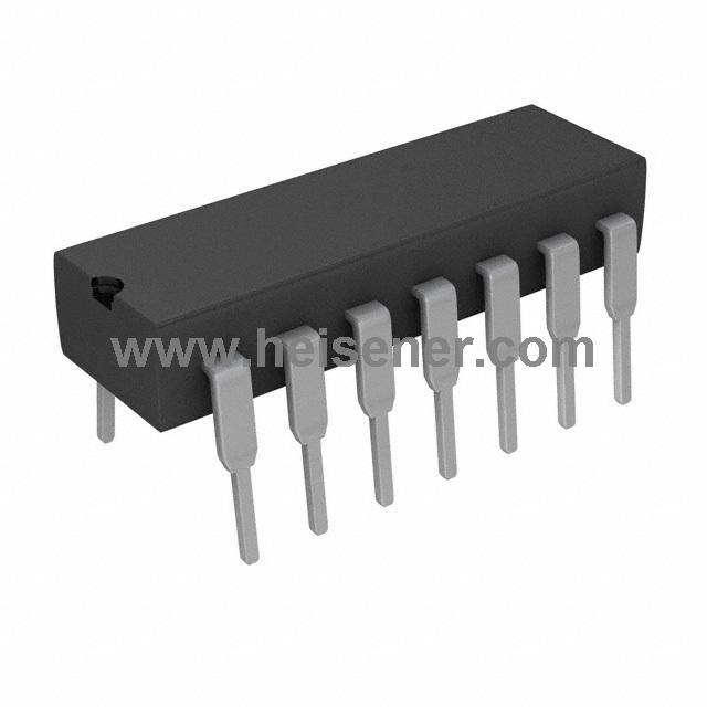
TLC274CN Introduction
The TLC274CN is a quad operational amplifier that offers a broad range of input offset voltage grades, low offset voltage drift, high input impedance, low noise, and fast response times, rivaling general-purpose BiFET devices. Built using Texas Instruments' silicon-gate LinCMOS™ technology, it provides excellent offset voltage stability, surpassing traditional metal-gate processes.
With extremely high input impedance, low bias currents, and high slew rates, the TLC274CN is a cost-effective alternative to BiFET and NFET products in various applications.
TLC274CN Symbol

TLC274CN Footprint

TLC274CN 3D Model

TLC274CN Pinout

OUT1: Output of the first operational amplifier.
IN1-: Inverting input of the first operational amplifier.
IN1+: Non-inverting input of the first operational amplifier.
VDD: Positive supply voltage for the IC.
IN2+: Non-inverting input of the second operational amplifier.
IN2-: Inverting input of the second operational amplifier.
OUT2: Output of the second operational amplifier.
OUT3: Output of the third operational amplifier.
IN3-: Inverting input of the third operational amplifier.
IN3+: Non-inverting input of the third operational amplifier.
GND: Ground (negative supply) for the IC.
IN4+: Non-inverting input of the fourth operational amplifier.
IN4-: Inverting input of the fourth operational amplifier.
OUT4: Output of the fourth operational amplifier.
TLC274CN Equivalent Schematic

TLC274CN Chip Info
These chips, when properly assembled, display characteristics similar to the TLC274C. Thermal compression or ultrasonic bonding may be used on the doped-aluminum bonding pads. Chips may be mounted with conductive epoxy or a gold-silicon preform.
TLC274CN Bonding Pad Assignments

TLC274CN Specification
| Parameter | Specification |
| Device Type | Quad Operational Amplifier |
| Technology | Silicon-gate LinCMOS™ |
| Offset Voltage | 1.1 mV |
| Input Bias Current | 0.6 pA |
| Supply Current | 2.7mA (x4 Channels) |
| Span Supply Voltage Range (Vdd) | 3V-16V |
| Input Impedance | High |
| Slew Rate | 3.6V/µs |
| Gain Bandwidth Product | 2.2 MHz |
| Operating Temperature | 0°C ~ 70°C |
| Package Size | 14-DIP |
| Status | Active |
TLC274CN Features
Trimmed Offset Voltage
Input Offset Voltage Drift, Including the First 30 Days
Wide Range of Supply Voltages Over Specified Temperature Range
Single-Supply Operation
Common-Mode Input Voltage Range Extends Below the Negative Rail (C-Suffix and I-Suffix Versions)
Low Noise
Output Voltage Range Includes Negative Rail
High Input Impedance
ESD-Protection Circuitry
Small-Outline Package Option Also Available in Tape and Reel
Designed-In Latch-Up Immunity
TLC274CN Applications
Precision Analog Signal Processing
Active Filters
Data Acquisition Systems
Comparators and Window Detectors
Instrumentation Amplifiers
Feedback Control Systems
Voltage Followers (Buffers)
Audio Amplification
Sensor Signal Conditioning
Voltage Regulation Circuits
Battery-Powered Applications
Automotive Applications
TLC274CN Package

How to Use TLC274CN?
When using the TLC274CN operational amplifier, the first step is to connect the power supply and ground. Connect the VDD pin to the positive power supply, typically +5V or +12V, and the GND pin to ground. After establishing the power connections, you can then connect the input signal to the appropriate input pin, such as IN1+ or IN1-, depending on whether you are using a positive or negative input. For multi-channel applications, you can connect additional input pins as needed.
Next, connect the output signal to the load or subsequent circuit to obtain the amplified signal. For example, the output of the first channel can be connected to OUT1 for further processing. If multiple channels are used, connect OUT2, OUT3, and OUT4 to obtain the respective outputs from each channel. Finally, to adjust the gain or frequency response, feedback loops can be configured using external resistors and capacitors.
FAQs
How can the gain of the TLC274CN be adjusted?
The gain of the TLC274CN can be adjusted using external resistors and capacitors in the feedback loop. By selecting appropriate values for these components, you can set the desired gain and frequency response for the amplifier.
Can the TLC274CN be used in both single and dual-supply configurations?
Yes, the TLC274CN is designed to work with both single-supply and dual-supply configurations, offering versatility in various circuit designs.
How does the TLC274CN compare to other operational amplifiers in terms of power consumption?
The TLC274CN offers low power consumption compared to conventional operational amplifiers, making it suitable for battery-operated and energy-efficient designs.