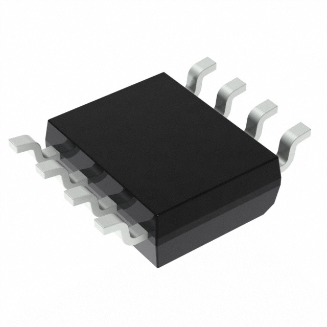
The CY2309 is a low-cost 3.3V zero-delay buffer designed to distribute high speed clocks in a 16-pin SOIC or TSSOP package. CY2305 is an 8-pin version of CY2309. It takes a reference input and drives five low-tilt clocks. The -1H version of each device operates at frequencies up to 100-/133 MHz and has higher drives than -1 devices. All parts have on-chip PLL that locks to the input clock on the REF pin.
Test Circuits

The PLL feedback is on-chip, obtained from the CLKOUT board. CY2309 has two groups, each with four outputs, which can be controlled by select inputs, as shown in the "Select Input decoding" table on page 3. If you don't need all the output clocks, BankB can say three things. Select input also allows the input clock to be applied directly to the output chip and for system testing purposes. CY2305 and CY2309 phase locked loops enter power-off mode when REF input end does not have rising edge. In this state, the output is three-state and the PLL is off, resulting in a current of less than 25.0 μA for these components.
The CY2309 PLL closes in another case, as shown in the table below. Multiple CY2305 and CY2309 devices can accept the same input clock and assign it. In this case, the tilt between the two device outputs is guaranteed to be less than 700ps. The CY2305/CY2309 is available in 2/3 different configurations as shown in the order information (page 10). CY2305-1/CY2309-1 is the basic component. The CY2305-1H/ CY2309-1H is a high-drive version of the -1, which has a much faster rise and fall time than the -1.
Logic block diagram
