L4970A Introduction
The L4970A is a highly efficient step-down power switching regulator capable of delivering up to 10A with an adjustable output voltage range from 5.1V to 40V. Utilizing BCD mixed technology and a DMOS output transistor, it achieves fast switching and low power loss. Features include reset and power fail for microprocessors, soft start, current limiting, and thermal protection.
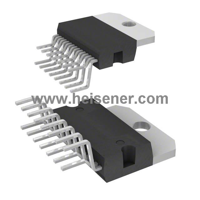
The device is housed in a 15-lead multiwatt package and requires few external components. Its ability to operate at switching frequencies up to 500kHz helps reduce the size and cost of external components, making it ideal for compact, cost-effective power regulation solutions.
L4970A Symbol

L4970A Footprint

L4970A 3D Model

L4970A Pin Connection

1. OSCILLATOR: Rosc. External resistor connected to ground determines the constant charging current of Cosc.
2. OSCILLATOR: Cosc. External capacitor connected to ground determines (with Rosc) the switching frequency.
3. RESET INPUT: Input of Power Fail Circuit. The threshold is 5.1V. It may be connected via a divider to the input for power fail function. It must be connected to pin 14 an external 30KΩ resistor when power fails signal not required.
4. RESET OUT: Open Collector Reset/power Fail Signal Output. This output is high when the supply and the output voltages are safe.
5. RESET DELAY: A Cd capacitor connected between this terminal and ground determines the reset signal delay time.
6. BOOTSTRAP: A Cboot capacitor connected between this terminal and the output allows the internal D-MOS transistor.
7. OUTPUT: Regulator Output.
8. GROUND: Common Ground Terminal
9. SUPPLY: VOLTAGE Unregulated Input Voltage.
10. FREQUENCY COMPENSATION: A series RC network connected between this terminal and ground determines the regulation loop gain characteristics.
11. FEEDBACK INPUT: The Feedback Terminal of the Regulation Loop. The output is connected directly to this terminal for 5.1V operation; it is connected via a divider for higher voltages.
12. SOFT START: Soft Start Time Constant. A capacitor is connected between the terminal and ground to define the soft start time constant.
13. SYNC INPUT: Multiple L4970A are synchronized by connecting pin 13 inputs together or via an external syncr. pulse.
14. Vref: 5.1V Vref Device Reference Voltage.
15. Vstart: Internal Start-up Circuit to Drive the Power Stage.
L4970A Block Diagram
The block diagram shows a DMOS power transistor with a PWM control loop, featuring a 5.1V ± 2% reference voltage, soft start, undervoltage lockout, current limit, thermal shutdown, and a reset/power fail circuit. The device turns on at 11V with 1V hysteresis. An external bootstrap capacitor, charged to 12V, provides gate drive for the DMOS transistor.
The circuit can source and sink peak currents up to 0.5A, supporting switching frequencies up to 500kHz. The PWM loop includes a sawtooth oscillator, error amplifier, comparator, latch, and output stage to generate a stable, fixed-frequency PWM drive, with a latch preventing multiple pulses even in noisy environments.

L4970A Circuit Operation
The L4970A is a 10A monolithic stepdown switching regulator working in continuous mode realized in the new BCD Technology. This technology allows the integration of isolated vertical DMOS power transistors plus mixed CMOS/Bipolar transistors.
The device can deliver 10A at an output voltage adjustable from 5.1V to 40V, and contains diagnostic and control functions that make it particularly suitable for microprocessor based systems.
L4970A Specification
| Specification | Value |
| Output Voltage Range | 5.1V to 40V |
| Output Current | 10A |
| Input Voltage Range | 15V to 50V |
| Switching Frequency | 200kHz |
| Package Type | 15-Multiwatt |
| Internal Transistor Type | DMOS |
| Line Regulation | Feedforward line regulation |
| Overcurrent Protection | Yes |
| Thermal Protection | Yes (Thermal shutdown) |
| Reset/Power Fail Output | Yes |
| Operating Temperature | -40°C ~ 150°C |
| Function | Step-Down |
L4970A Features
10A Output Current
5.1V to 40V Output Voltage Range
0 to 90% Duty Cycle Range
Internal Feed-Forward Line Regulation Internal Current Limiting
Precise 5.1V ± 2% on Chip Reference
Reset and Power Fail Functions
Soft Start
Input/Output Sync Pin
Under Voltage Lock Out With Hysteretic Turn-On
PWM LATCH FOR SINGLE PULSE PER PERIOD
VERY HIGH EFFICIENCY
SWITCHING FREQUENCY UP TO 500KHz
THERMAL SHUTDOWN
CONTINUOUS MODE OPERATION
L4970A Applications
Microprocessor Power Supplies
Industrial Equipment
Telecommunications Equipment
Automotive Power Supplies
Power Management in Battery-Operated Devices
Power Supplies for LED Drivers
Test and Measurement Equipment
L4970A Package

L4970A FAQs
What external components are required for the L4970A?
The L4970A requires only a few external components, primarily for filtering and setting the output voltage. This helps minimize complexity in your design.
What is the typical efficiency of the L4970A?
The L4970A offers high efficiency due to its DMOS output transistor, with typical efficiency exceeding 90%.
What is the typical start-up behavior of the L4970A?
The L4970A includes soft start functionality, which reduces inrush current during power-up, preventing voltage overshoot and damage to components.