Is AI the killer application that will enable widespread adoption of silicon photonics? One would think so, given the explosive growth in AI over the last couple of years driving the need for high-speed interconnections and higher bandwidths, and subsequently Ethernet optical transceivers.
This was the question addressed at an industry workshop in March in San Diego, Calif., by Soitec and CEA-Leti—co-chaired by Nvidia—followed by a panel moderated by EE Times as the exclusive media partner. Running on the sidelines of the Optical Fiber Communications (OFC) Conference exhibition, speakers from LightCounting, Jabil, TSMC, Google, and Nvidia presented the case for silicon photonics for delivering the massive data transport and processing requirements of AI in cloud data centers, as well as enterprise and telecoms networks.

AI has doubled the market for Ethernet transceivers in just two years, and volumes are expected to double both this year and in 2025. (Source: LightCounting)
According to LightCounting’s data, AI has doubled the market for Ethernet transceivers in just two years, and volumes are expected to double both this year and in 2025. Optics could play a key future role, but power consumption of optical connectivity would need to be reduced. LightCounting founder and CEO, Vladimir Kozlov, said 50GW is currently enough to support all hardware in cloud data centers as of 2023. But this will increase to more than 150GW by 2029.
It was clear from the presentations that we are at a potential turning point for silicon photonics. But there were still challenges in terms of scaling, energy efficiency, packaging, ecosystem, and tools like EDA and third-party IP, as well as materials.
Packaging and EDA particularly dominated the discussion.
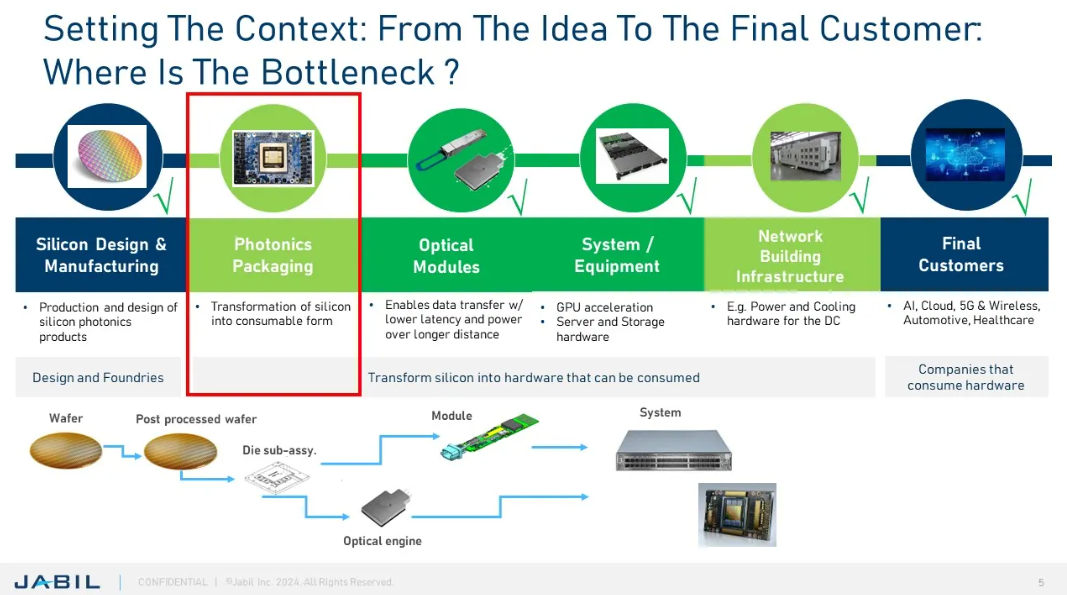
On packaging, Giorgio Cazzaniga, director of product management and development at Jabil, said there is a need for a manufacturing photonics packaging process with large-scale manufacturing capabilities in place. He said that silicon photonics entry costs are currently low due to availability of pilot lines for prototyping.
“What happens when a solution is needed for the production for thousands or millions of pieces to satisfy AI numbers?” Cazzaniga asked.

Silicon photonics packaging needs to be predictable and scalable and is the current bottleneck. (Source: Jabil)
He pointed out the commonalities of the silicon photonics packaging process and chiplets.
“Chiplet architecture presents the possibility to have different chips—designed with technologies specialized for different tasks like memory, computing, acceleration—on the same interposer,” Cazzaniga said. “A chiplet can be a silicon photonics PIC that could be integrated on the same substrate as any other. From a packaging point of view, chiplet architecture requires some steps (flip chip, bonding, etc.) that are also needed for photonics packaging activities. However, photonics chips require specific steps such fiber attachment.”
The fiber attachment challenge, in terms of both reliability and scaling, was highlighted by most of the speakers. However, Cazzaniga commented that photonics packaging needed to evolve from being “handmade” to being a fully automated process to handle the high-volume demand from AI.
“This requires investment into automation—some shared with chiplet packaging—to reduce the overall production time and finally minimize cost,” he said.
In this respect, the speakers generally highlighted that for AI to become a killer application, silicon photonics must be practical in deployment, cost-efficient, reliable (or at least have a predictable reliability), serviceable, and scalable.
In the audience, a key point made was in regard to the EDA tools challenges: you cannot yet predict right first-time designs. There is a lack of something like SPICE for photonics, where you have a standard modelling package that all tools can support—say, to have standard models for modulators that you can slot into your parameters, and get right-first time prediction of what your design is going to do.
Then you need to be able to plug in variability into the model to predict what your device is going to do. And finally, you’ll need digital twins of not just the component, but also the environment, so that it is possible to make sure all elements of the design work together.

Silicon photonics is increasingly being adopted in transceivers. (Source: LightCounting)
So, what are likely to be the trigger points for widespread adoption? Most of the speakers were in consensus that the key will be scale of integration for silicon photonics. They said that more standardization of packaging would be desirable, as would the development of an ecosystem for optics generally as there is for electronics. Tackling power consumption would also be important.
They concluded that decisions of big companies or big customers will really be the key driver of silicon photonics for AI.
About US
