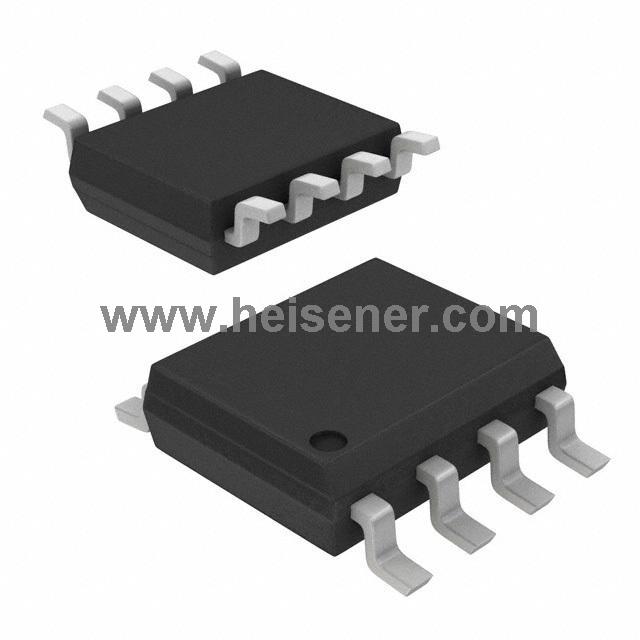
The FDS4435BZ is a P-Channel MOSFET built with Fairchild Semiconductor’s PowerTrench® technology, designed to keep on-state resistance as low as possible. It is a great choice for power management and load switching in devices like laptops and portable battery packs. Its efficient design helps improve overall performance while keeping energy losses to a minimum.

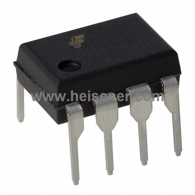
Pins 1, 2, 3 → Source (S): These pins are connected together and serve as the source terminal where current enters the MOSFET.
Pin 4 → Gate (G): This pin controls the MOSFET’s switching operation by applying a voltage to turn it ON or OFF.
Pins 5, 6, 7, 8 → Drain (D): These four pins are connected together and serve as the drain terminal, where current exits the MOSFET when it is conducting.


| Parameter | Value |
| Drain to Source Voltage (Vdss) | 30V |
| Current - Continuous Drain (Id) @ 25°C | 8.8A (Ta) |
| Continuous Drain Current (ID) | -8.3A (TA = 25°C) |
| Drive Voltage (Max Rds On, Min Rds On) | 4.5V, 10V |
| Rds On (Max) @ Id, Vgs | 20mOhm @ 8.8A, 10V |
| Vgs (Max) | ±25V |
| Vgs(th) (Max) @ Id | 3V @ 250µA |
| Gate Charge (Qg) (Max) @ Vgs |
40 nC @ 10 V |
| Input Capacitance (Ciss) (Max) @ Vds | 1845 pF @ 15 V |
| Power Dissipation (Max) | 2.5W (TA = 25°C) |
| Package Type | 8-SOIC |
Max rDS(on) = 20m at V GS = -10V, ID = -8.8A
Max rDS(on) = 35m at V GS = -4.5V, ID = -6.7A
Extended V GSS range (-25V) for battery applications
HBM ESD protection level of ±3.8KV typical (note 3)
High performance trench technology for extremely low r DS(on)
High power and current handling capability
Termination is Lead-free and RoHS compliant
Power Management
Load Switching
Notebook Computers
Portable Battery Packs
DC-DC Converters
Here are 5-6 alternatives to the FDS4435BZ below:
FDS4435
FDS4435A
FDS4435B
IRLZ44N
AO3400A
STP55NF06L


First, identify its three pins: Gate (G), Drain (D), and Source (S). The Source typically connects to the positive voltage supply (Vcc), while the Drain goes to the load. The Gate controls the MOSFET—when you apply a low voltage (close to ground) to it, the MOSFET turns on, allowing current to flow from Source to Drain. Conversely, when the Gate is at the same voltage as the Source, the MOSFET turns off.
Now, for a practical setup: if you're using it as a switch, connect the Drain to one side of your load and the Source to Vcc. Then, use a pull-up resistor (typically 10kΩ to 100kΩ) to keep the Gate high when not actively driven. Finally, control the Gate with a low-side switch, such as a microcontroller output. This way, pulling the Gate low turns the MOSFET on, and releasing it (allowing the pull-up to bring it high) turns it off.
The FDS4435BZ is a P-channel MOSFET designed for switching applications. It features low on-resistance (R_DS(on)), fast switching speed, and is commonly used in low-voltage, high-current circuits.
Since it’s a P-channel MOSFET, connect the Source to the positive supply (Vcc) and the Drain to the load. To turn it ON, apply a low voltage to the Gate (near ground). To turn it OFF, pull the Gate to Vcc (usually using a pull-up resistor).
The FDS4435BZ is an improved version of the FDS4435, featuring better thermal performance and slightly lower on-resistance (R_DS(on)), making it more efficient in power management applications. However, both share similar electrical characteristics and can often be used interchangeably.