The latest 5G standard specification published by 3GPP formalizes and improves many features that increase the utility and complexity of 5G hardware. Mobile broadband Augments (eMBB), Ultra-reliable low-latency communications (URLLC), massive machine-type communications/Massive Internet of Things (mMTC/mIoT), and enhanced certainty all bring unique aspects to 5G wireless communications, combining the capabilities of highly specialized priority systems into a single standard with global reach.
Another novelty of 5G is that, with the opening up of frequency selection and the application of cellular communication technologies at these frequencies, 5G will incorporate bands in the millimeter wave (mmWave) spectrum, possibly up to 90GHz.
All of these new features and capabilities of 5G change the cellular connectivity paradigm, making it the voice, text and Internet data platform for mobile phones. This makes 5G an even more ubiquitous wireless communication and connectivity solution for a variety of medical, industrial, government, military, automotive, aerospace, security, big data, and other emerging applications.
5G antenna module
These new 5G use cases and capabilities change the landscape of 5G antenna modules from dedicated, often custom designed and developed portable mobile device hardware used in smartphones and tablets. This translates into integrated iot modules in sensor platforms, autonomous mobile robots (AMR), industrial control devices, augmented reality/virtual reality (AR/VR) headsets/systems, and automotive platforms.
Taking the latest version of 3GPP (release 17) as an example, the 64T64R has a 16-layer downlink (DL) and an 8-layer uplink (UL). It is ideal for 256 antenna elements or 16×16 designs. In comparison, 4G has a maximum MIMO capability of 8T8R DL and 4T4R UL. As a result, with the release of the latest 5G version, the total number of antenna elements and MIMO layers has increased dramatically.
This has led to major shifts in the design of antenna modules, radio frequency front end (RFFE) modules, MIMO/ beamforming signal processing and cabling complexity. This level of complexity and increased wiring density is beyond the capabilities of traditional PCB technology.
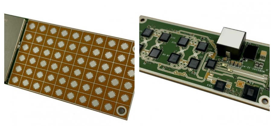
Figure 1: 5G antenna modules are moving from custom-designed hardware to iot modules serving a variety of 5G applications

For some time now, a similar technological trend has been emerging in the field of satellite communications (Satcom). A common solution for satellite communications to these challenges is highly complex custom panels made of stacked circuit boards, often with embedded components. Now, people are exploring in-board or on-board antenna technology for 5G base station units from macro stations to small base stations.
However, this solution often involves specialized processes, resulting in relatively low yields and is not suitable for mass production of 5G antenna modules to meet the growing demand for 5G connectivity solutions. In addition, these panel solutions are large compared to typical iot antenna module sizes, which are mostly just a few centimeters in side length.
Encapsulated antenna
5G antenna modules require new solutions to meet the demands of new 5G applications. Therefore, chip and module encapsulation technologies have been studied for antenna in package (AiP), antenna on package (AoP), antenna on chip (AoC) and other integrated 5G antenna modules.
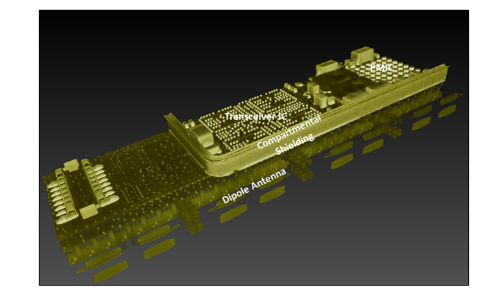
Figure 2: AiP can integrate one or more antennas into an IC package with RF chips such as transceivers

In order to achieve the goal of manufacturing 5G antenna modules that are compact, relatively low cost, easy to mass produce, and in sufficient quantities, many approaches are being explored. Some of these approaches include placing the antenna module as a small chip in a system-level package (SiP), and some even integrate the antenna as a system-on-chip (SoC) into the IC itself.
For example, AoP technology is integrated with an antenna module at the top of a SiP package, perhaps as part of a shell, shield, or as an add-on board stacked on top of or next to other small chip or board modules.
A key consideration in all of this work is the performance of the individual antenna elements and the entire antenna module. Antenna performance depends on subtle design features, as well as the relative size of the conductors proportional to the wavelength of the electrical signals stimulating the antenna elements. In general, the larger the antenna, the greater the electrical length and the higher the gain.
There are ways to artificially increase electrical length through resonant elements, fractal design techniques, and other techniques. Many of these methods produce good narrowband antenna performance, but can also be tweaked to achieve enhanced broadband performance. However, these methods all greatly increase the complexity of the antenna element, which increases the cost, development time, and reduces the possible yield.
Many modern array antennas are made up of patch antennas that are either converted or some variant of a phased array. Therefore, the challenge is how to achieve a high level of antenna efficiency and gain using a small patch antenna array on a compact IC or SiP. The answer is simple, much of the effort in developing AiP, AoP, and AoC has been for operation at millimeter-wave frequencies, where relative wavelengths enable reasonable antenna efficiency in a compact size.
A set of relatively small antenna elements can be used as an array to effectively combine the antenna elements into a single larger antenna. This approach does not take advantage of MIMO, but is compatible with beamforming and allows more compact antennas to operate at lower frequencies.
Antenna on chip
One of the challenges of the AiP/AoP/AoC approach is how to achieve extremely high density interconnects with very small spacing and occupying area. With IC technology, this can be handled with existing IC wiring functions, but it may be advantageous to use different semiconductors for antenna modules and RFFE. In this case, 2.5D or even full 3D IC technology may be required to enable the stacking or tight integration of various semiconductor materials and processes to combine RF and digital electronics.
Currently, there are some relatively mature 2.5D and 3D IC technologies, but most of these mature technologies are used in pure digital circuits such as memory, storage, GPU, CPU and FPGA. There are some commercial products that combine RF and digital circuits in this way, but these products are still very proprietary and not widely used.
If these design and integration challenges can be solved, then the miniaturization of 5G antenna modules will bring huge benefits. This includes having more compact 5G antenna modules that are potentially more efficient, less costly, easier to mass produce, and can be pre-certified in efficient automated test facilities.
Figure 3: 5G antenna solutions are likely to grow in density and miniaturization
 Simplifying the Bill of materials (BOM) and component procurement is extremely advantageous for businesses trying to rapidly develop 5G technology, especially since standards and certification requirements are constantly changing and volatility is likely in the coming period as millimeter wave technology becomes more widely available.
About US
Heisener Electronic is a famous international One Stop Purchasing Service Provider of Electronic Components. Based on the concept of Customer-orientation and Innovation, a good process control system, professional management team, advanced inventory management technology, we can provide one-stop electronic component supporting services that Heisener is the preferred partner for all the enterprises and research institutions.
