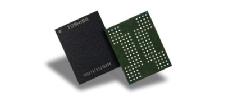
The prototype chip uses the same processing technology as 64-layer 3D NAND and stores 768Gb / 96GB data.
Beginning in early June, shipping prototypes to SSD and SSD controller vendors for evaluation and development.
QLC 3D flash memory enables 1.5 TB (TB) devices in a single package. The device has a 16-die stacked architecture, which is the industry's largest capacity.
Toshiba has mass-produced 64-layer 256Gb / 32GB devices.
Toshiba has also developed prototype samples of 96-layer 3D NAND using three-level cell (TLC) technology. Samples are scheduled for release in the second half of 2017, and the volume production target is 2018.
The 96-layer process is expected to deliver 512Gb equipment in the near future and use 4-bit (quad-level cell, QLC) technology per cell.
This 96-layer TLC chip will be manufactured on February 5th, the new February 2nd and February 6th in Yokkaichi, and will open in the summer of 2018.